How do Strategic Cooperation with Suitable Plans can help the Japanese Semiconductor Industry

Under high market demand of automobile, consumer and Information and Communication Technology (ICT) chips due to COVID-19 and development of smart driving, Japanese Semiconductor Industry is facing both chances and also challenges. In my opinion, for better future Japanese Semiconductor Industry, it is essential to achieve these two targets listed below.

  1. New Japanese semiconductor production and test equipment developed for satisfactory yield rate (>90%) and lower production cost when using advanced process. (Plan A1)
  2. Japanese firms can carry out strategic cooperation with universities and companies (Can be foreign), for development of new semiconductor devices and more advanced process (40nm below). These researches are carried out using current semiconductor production systems. As a result, relative Japanese firms also can also produce these new devices themselves. (Plan A2)

Both of Plan A1 and A2 can be carried out at the same time to help the Japanese Semiconductor as much as possible. This article discusses how strategic cooperation with suitable plans can help the Japanese Semiconductor Industry. Before explaining my views about details of strategic cooperation, let me tell you what is the importance of strategic cooperation for better future of Japanese Semiconductor firms.

For Plan A1, I have written an article entitled “Winning the Semiconductor War by a Foundry with Specific Process”.  This approach aims to use patents, engineers and foundries from TPSCO to help Japanese Firms. In the future, Japanese new technologies and equipment can also be applied by X in developing new semiconductor process, with lower production cost [1], shorter lead time [2] and higher yield rate [3]. Currently, technical solutions newly developed by Japanese firms such as Jet and Flash Imprint Lithography (J-FIL) [3] and Minimal Fab [2] have much less practical experience. That results in long time preparation for them to be ready to compete with their foreign competitors such as ASML. TPSCO also currently cannot produce chips using process less than 45nm [4]. Some people suggest outsourcing more chip production to pure foundries such as TSMC and UMC.

However, on-going global shortage in wafer production capacity is due to the sharply increasing in demand of ICT (Including 5G Communication) systems and chips due to the pandemic and the recovering automobile market [5, 6, and 9]. Consumer and ICT Chips also have higher marginal profit and demand than those of automobile chips for TSMC [7, 8]. The global automobile market has been shrunk for about two years [5]. Hence, the original capacity for automobile chips has been also used by chips for consumer and ICT applications.

Due to the development of smart driving and electric vehicle, much more chips will be used by cars [5, 9]. USA, Germany and other countries have urged Taiwanese foundries to offer more wafer production capacity for automobile semiconductor [10, 11]. For major players such as Renesas, which need TSMC on production of chips using 40nm and smaller CMOS process [12, 13]. Renesas has been forced to use more production lines in Naka Fab for 40nm chip production [14]. According to some experts, including Jason Wang (CEO of UMC) and Hidetoshi Shibata (CEO of Renesas Electronics), said the shortage of automobile chips will last for at least several months, or even longer [9, 15 and 16]. Change of foundries can cause serious difficulty in on – time delivery and quality control of chip production. In the foreseeable future, China‘s military expansion against Taiwan will be another threat on stability of TSMC wafer production so the Japanese government might then have tried to invite TSMC to set up new fabs in Japan [17].

However, it is not feasible for inviting TSMC to set up new fabs in Japan. North America companies such as Qualcomm, Xilinx, AMD, Nvidia and Apple have contributed about 60% of TSMC total income [18, 19] in recent years. However, only about 5 -6% of TSMC total Income has been from Japan [18, 19]. 3 of Top 5 major manufacturers of semiconductor equipment also come from America [20, 21]. Synopsys and Cadence, two of the top three software companies offering IC Design package, also come from America.

As a result, that states the importance of Plan 1B. It helps in getting engineering knowledge of new devices and processes. That makes Japanese Semiconductor Industry know what technological requirements are essential in production of new chips and devices. By cooperation with some selected foreign companies, more technical details and process can be learnt for training of Japanese companies and engineers. After that, it will also be helpful for later modification of J-FIL and Minimal Fab. Details about cooperation between foreign firms and Japanese companies will be described in the following paragraphs. In my opinion, there are two ways.

  1. Renesas Electronics can work with UMC regarding the Deeply Depleted Channel™ (DDC) process, which is useful in chips with ultra low power consumption. After that, Renesas can manufacture chips using DDC technology at its fab (Plan 1B-1).
  2. University of Tohoku, Kioxia and Sony can also cooperate for SOT- MRAM, used in cache memory of advanced CIS and memory chips (Plan 1B-2).

For Plan 1B-1, UMC gradually licenses its 28nm and below semiconductor process platform to Renesas. After Renesas has feminized with 28nm semiconductor process platform, UMC then outsources the development of automobile grade DDC CMOS process (40nm and below) to Renesas. Finally, the results of DDC technology development will be shared by both UMC and Renesas. A Win – Win situation can be achieved between UMC and Renesas.

  1. UMC also needs to focus its effort and resources on modification of 14nm CMOS Process. For foundries, more micro – refined process is more profitable than that of less micro – refined process. Let‘s take TSMC as an example.
Chart 1: Wafer Revenue by Technology over Quarters of TSMC (Data from TSMC website [8])

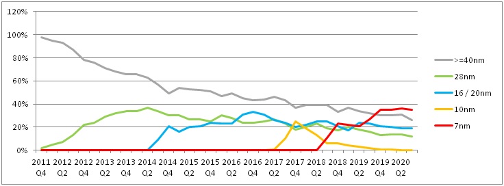
According to Chart 1, if a newer process has higher revenue than others, it will take shorter time to achieve a specific sufficient percentage (In this article, 33% is selected as reference). For TSMC 28nm CMOS Process, it takes 27 months to contribute about 33% of total wafer revenue at a later quarter. However, it only took 18 months for TSMC 7nm CMOS Process to achieve the same target. Higher wafer revenue of for TSMC 7nm CMOS Process is due to the global wafer foundry market has become a duopoly. Only Samsung and TSMC have enough capital and technical assents to invest in more micro-refined semiconductor process. According to the third quarter of 2020, 20nm and below CMOS process has contributed over than 50% of TSMC total income [8]. If UMC staff can focus on its 14nm CMOS process modification earlier, which is more profitable, its operation efficiency and R&D progress can be further improved.

  • It results in more stable fab network and more advantage in R&D of Renesas chips. Renesas will have more advantage in developing chips. Currently, Renesas‘s SOTB Process has been developed due to its ultra low power consumption [22]. However, when the SOTB process is further miniaturized from 65nm, thinner wires result in larger leakage current. Finally, 28nm SOTB will have no technical advantage over 28nm FD-SOI because their leakage current is close to each other [23]. In my opinion, DDC is a better alternative for Renesas because it slightly modifies conventional planar bulk CMOS transistors by changing the single CMOS channel layer into three functional layers [26, 27]. The diagram of a DDC transistor is shown in Figure 2.
Figure 2: Diagram of a DDC transistor [25 – 28] (Source: SuVolta via https://ascii.jp/elem/000/000/898/898862/3/)

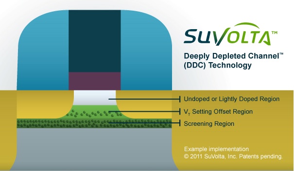
From Figure 2, the features of three layers within channel layer are shown below.

Top layer (Undoped or lightly Doped): Enable Vdd scaling and transistors driving larger effective current [26, 27]

Middle layer (Vth setting and Vth variability suppression of transistors): It aims to better yield (For random dopant fluctuation (RDF) reduction [27]) and identical speed of all transistors [26]) without degrading channel mobility [26, 27].

Bottom layer (Screening): Body for its depleted behavior (For achieving many merits compared to planar bulk CMOS [24]) as that of SOTB transistor and further dynamic Vth variability suppression through biasing [26, 27]

Further power saving and temperature effect minimization can be achieved by dynamic body biasing on the body layer, underneath of the three channel layers of Figure 2 [25, 28]. DDC PowerShrink technology enables power saving by 50% and reduction of supply voltage (Vdd) by 30% [25, 26, 28] while original clock speed can also be maintained.  Standard planar bulk CMOS design and manufacturing infrastructure can be slightly modified to produce chips using DDC PowerShrink transistors [25, 26]. Expected features of DDC PowerShrink technology has been obtained using a 28nm transistor (Effects of DDC on 14nm CMOS process has been confirmed by simulation [28]). As a result, DDC can become a better alternative apart from FD-SOI and Fin-FET which require expensive investment in special process and manufacturing systems [25, 28]. DDC PowerShrink has been firstly adopted at a mass production of Fujitsu Semiconductor MB86S22AA, an image processor on 2013 (Source: https://www.fujitsu.com/jp/group/fsl/en/documents/about/resources/news/press-releases/2013/20130904-2e.pdf).By adopting DDC PowerShrink technology, Renesas‘s chips can achieve ultra low power consumption and lower cost.

  • It will be helpful to feminize clients with advantages of new technology developed by Renesas and UMC. If DDC CMOS technology can be adopted by Renesas, more Japanese clients can be attracted to use DDC PowerShrink technology and outsource their chip production to UMC.
  • Some people may think that Renesas can also become another competitor of UMC after it can use 28nm CMOS process to manufacture chips. However, in my opinion, UMC and Renesas can achieve a Win – Win situation by my idea.
  • Renesas can share the results of R&D with UMC and its expenditure can be shared with UMC and INCJ
  • UMC does not compete with its clients because UMC just have revenues by its wafer foundry service. However, Renesas competes with many other semiconductor firms, which may be clients of UMC.
  • UMC has more micro-refined process technology (14nm currently) than Renesas (40nm minimum currently [29])

By strategic cooperation with UMC, Renesas can co-develop and produce chip itself using DDC ultra low power. Apart from sharing DDC technologies with Renesas, UMC also can utilize its resource on other useful technologies.

After Plan 1B-1, the paragraphs below will explain Plan 1B-2.      

For Plan 1B-2, Because of large demand of CIS from smart devices and CCTVs, Sony can get large amount of income from their CIS products [30, 31]. Sony even has invested more on R&D of CIS [31, 32]. Samsung, second major supplier of CIS, has also started the transformation of its old fabs, for producing more new CIS [31, 32]. It shows that CIS market is profitable with satisfactory margin profit. It can attract Sony to invest more money on CIS development. Sony has developed the first 3-Layer, 960 fps CMOS Image Sensors (CIS) for [33]. This CIS enables super slow motion Full HD (1920 x 1080 pixels, up to 960 fps) movies and high speed readout of pixel data (19.3M pixel in 1/120 second). This image sensor also requires DRAM for temporarily storing the high speed pixel data [33] during taking super slow motion movie (in Full HD). However, for further development of CIS, it is essential for CIS manufacturers to deal with higher pixel data rate for applications such as 8K filming, gaming and sporting applications, which need high Frame per Second (FPS) videos for eliminating motion blur and maintaining the video quality at super slow motion screening [34]. Due to increasing number of pixels of CIS, more micro refined process also has been adopted in development of CIS [34]. As a result, a type of new memory for temporary storage of pixel data must have better scalability and higher speed than those of DRAM.  STT-MRAM is being a candidate of new generic memory due to its capability of downscaling [36], non-volatility [35, 36, 37, 38], lower power consumption [35, 36, 37], less complexity [37], immune to radiation [37], higher density [35], number of rewrites [35] and faster R/W speed [35, 36, 37, 38].

However, the write speed of STT-MRAM is currently not fast enough to be next generation of cache memory due to its design [35, 39, and 40]. The read and write operations are controlled by the same path [39], which results in larger write latency and slower write speed. For further higher writing speed, SOT-MRAM has been developed for new L1 / L2 cache memory. Researchers of Tohoku University has also developed SOT-MRAM memory cell using standard 55nm CMOS process, with demonstration of sub-ns write speed and semiconductor integration process for SOT-MRAM, enabling thermal tolerance against 400 Degrees annealing [40] during standard semiconductor production. Sony has used Micron DRAM as temporary storage of pixel data [33] but SOT-MRAM can be used as temporary memory for Sony CIS in the future.

Kioxia can also produce SOT-MRAM for Sony CIS and its own memory products, used as high speed memory in both caches and solid state disk (SSD). Due to its high speed, high density and other advantages, Kioxia will become a potential strong opponent of current DRAM main manufacturers. 

Finally, this article has shown my ideas of suitable plans of strategic cooperation, which are essential for future success of the Japanese Semiconductor Industry. I also will be glad if my ideas and opinion can help Japanese Semiconductor Firms to strike a good balance between cost control and more stable supply of their chips by extra investment on their fabs.

References

[1] cnt.canon.com/technology/j-fil-overview/

[2] https://report.nat.gov.tw/ReportFront/PageSystem/reportFileDownload/C10603764/001

[3] https://www.nature.com/articles/micronano201775.pdf

[4] https://tpsemico.com/process_technology_offerings/

[5] https://www.bnext.com.tw/article/61163/car-chip-global-problem?utm_source=dable

[6] https://money.udn.com/money/story/5612/5240010?from=edn_catehotlist_story

[7] https://ctee.com.tw/news/stock/412893.html

[8] TSMC Financial Report https://investor.tsmc.com/chinese/quarterly-results

[9] https://www.moneyweekly.com.tw/ArticleData/Info/說解財經大小事/52325/

[10] https://www.reuters.com/article/us-taiwan-autos-chips/germany-urges-taiwan-to-help-ease-auto-chip-shortage-idUSKBN29T04V?il=0

[11] https://www.bloomberg.com/news/articles/2021-01-29/u-s-officials-to-press-taiwan-tsmc-to-resolve-auto-chip-crunch

[12] https://www.renesas.com/us/en/about/press-room/renesas-electronics-and-tsmc-announce-28nm-mcu-collaboration-next-generation-green-and-autonomous

[13] https://pr.tsmc.com/chinese/news/1903

[14] https://cn.nikkei.com/industry/itelectric-appliance/43647-2021-01-29-08-48-59.html/?n_cid=NKCHA014

[15] https://www.bloomberg.com/news/articles/2021-03-12/carmakers-chip-shortages-may-last-into-late-2021-renesas-says

[16] https://news.cnyes.com/news/id/4562881

[17] https://www.bnext.com.tw/article/61224/japan-semiconductor-tsmc?utm_source=dable

[18] https://finance.technews.tw/2019/02/23/tsmc-2018-market/

[19] https://investor.tsmc.com/static/annualReports/2019/chinese/pdf/c_all.pdf

[20] https://www.vlsiresearch.com/the-chip-insider/semiconductor-equipment-suppliers-growth-database-2019

[21] https://www.vlsiresearch.com/public/cms_pdf_upload/tci190314/tci190314.htm

[22] https://www.renesas.com/us/en/solutions/key-technology/sotb/merit.html

[23] http://eetimes.jp/ee/articles/1811/20/news041_2.html

[24] https://www.soitec.com/en/products/fd-soi

[25] https://www.printedelectronicsworld.com/articles/3471/suvoltas-innovative-powershrink

[26] https://www.electronicdesign.com/technologies/digital-ics/article/21794530/how-deeply-depleted-channel-transistors-work

[27] https://www.theregister.com/Print/2011/12/07/suvolta_ddc_transistor/

[28] https://news.mynavi.jp/article/20110616-powershrink/

[29] https://www.sangyo-times.jp/article.aspx?ID=3138

[30] https://www.reuters.com/article/us-sony-results/sony-surprises-with-record-profit-as-image-sensor-demand-offsets-weak-gaming-idUSKCN1UP0FQ

[31] https://udn.com/news/story/7240/4680936

[32] http://www.businesskorea.co.kr/news/articleView.html?idxno=56553

[33] https://fuse.wikichip.org/news/763/iedm-2017-sonys-3-layer-stacked-cmos-image-sensor-technology/

[34] https://camerajabber.com/buyersguides/which-cameras-shoot-4k-at-120fps/

[35] https://pc.watch.impress.co.jp/docs/column/semicon/1145577.html

[36] https://news.cnyes.com/news/id/4468534

[37] https://www.spinmemory.com/spinuploads/2018/07/IT-ProPortal-eprint-MRAM_plain_v2.pdf

[38] https://www.eettaiwan.com/20190314nt22-most-mram/

[39] https://www.digitimes.com.tw/col/article.asp?id=1017

https://www.digitimes.com.tw/col/article.asp?id=1018

[40] https://www.tohoku.ac.jp/en/press/sot_with300mm_si_cmos_technology.html

Winning the Semiconductor War by a Foundry with Specific Process

Nowadays, due to challenging competitors and the changing global semiconductor market, many semiconductor firms such as Qualcomm, Socionext and NXP, do not own any foundries for minimizing their operation cost. They outsource their chip production to foundries such as TSMC, GlobalFoundries (GF) and UMC. However, among major players in the global semiconductor market, such as Samsung, Micron and Intel, with many CMOS process patents and technical advantages, still have their foundries. Their production experience and CMOS process technologies can still be useful in narrowing the gap between themselves and their fabless opponents.

Among these major players with fabs, many of them such as Sony, Renesas and Rohm are Japanese firms, which products are competitive in markets of specially semiconductor products with higher margin profits [1, 2, 3, 4, 5, 6] such image sensors [1, 2], microcontrollers [3, 4, 5] and discrete power semiconductor component [6] respectively. That means becoming fabless helps but not guarantees to win in competition in the global semiconductor market. These major Japanese players with fabs need alternative support for their success in the future.

In this article, a joint foundry company, called X, is planned to be established. X will help Japanese semiconductor companies to be winners in the future.

How will X be established? In my opinion, by firstly acquiring 49% of TPSCO (Towerjazz Panasonic Semiconductor Co., Ltd) from Panasonic, then negotiating with Towerjazz from setting up a Joint Venture called X. X will keep all assets of TPSCO including its three manufacturing facilities and Technical Patents. The arrangement of shares of X among Towerjazz, the Japanese Government (INCJ or DBJ) and other Japanese firms follows the previous agreement of the sale of the Toshiba Memory Corporation (TMC) (Now called Kioxia) [7]. That means Towerjazz, will become the major shareholder and have 49% of X share and the Japanese Government (INCJ or DBJ) and other Japanese firms will have the rest 51% of X share. That means the Japanese still control X. Extra financial and technical support can be helpful to persuade Towerjazz to reach an agreement about X with the Japanese Government.

Why choosing TPSCO but not other fabs? The next few paragraphs will explain about this.

Firstly, many major Japanese players have advantages in specific semiconductor devices market. Sony CMOS Image Sensors (CIS) have dominated the global CIS market [8]. Image Sensor is a rectangle but Wafer is circular. As a result, wafer area cannot be fully utilized. For producing Image Sensors with the same size of wafer, more wafer area will be wasted if the sensor area is larger. That result in extremely high pixel yield rate requirement in production [9]. Because of large demand of CIS from smart devices and CCTVs [10], Sony can get large amount of income from their CIS products [11]. Two more 300mm fabs have also been acquired by Sony for higher production capacity of CMOS Sensors [12, 13, and 14]. Renesas has begun their usage of their ultra low power 65nm Silicon on Thin Buried Oxide (SOTB) process in one of their MCUs [15]. SOTB process, a specific SOI CMOS process, achieves ultra low power consumption [16]. That will be suitable to chips used in energy harvesting applications and IOT (Internet of Things) Devices, work for long time without batteries. SOI chips fulfil low power consumption with less initial investment in more advanced micro – refinement technology [17, 18]. That provides semiconductor firms with more cost – effective technical platform for their devices. GF even develops and produces chips using its fully depleted SOI process [19]. Integrated Power devices can also be widely used in various applications such as future electric vehicles and trains [20]. They need alternative technical support for accelerating their research and development (R & D) process for lower power dissipation and lower production cost. TPSCO is a successful foundry which provides special CMOS process solutions, used in Image Sensors, Low power Silicon on Insulator (SOI) and Power devices [21]. The competitiveness of TPSCO is based on its relative technical patents and professional R&D engineer.

By licensing TPSCO technical patents to major Japanese semiconductor players, they will be capable for rolling out their products more quickly. Earlier release of products is a key factor of victory in the global semiconductor market.

Some people may think that the technical patents licensed from X may be easily leaked. However, X can minimize the risk of technical secret leakage by measures such as Non – Disclosure Agreement (NDA). Japanese Companies can also be requested to produce their products using patents from X at their designated fabs in Japan only.

Secondly, TPSCO has manufacture experience of image sensors, SOI chips and integrated power devices. Its staffs also have experience of using patents licensed by clients in semiconductor production. X is a pure wafer foundry player, which only obtains income by its foundry service. Semiconductor firms do not need to worry that X will compete against them [22]. They can also freely to license their patents to X for production of their specific chip products. By offering wafer foundry service to these firms, the production cost of Japanese semiconductor firm can also be reduced. As a result, their products can be more competitive.

Thirdly, previously, the Panasonic Corporation (Panasonic) was actively developing the more micro – refined CMOS process [23]. However, due to its huge financial loss in 2013, its fabs have been sold to TPSCO, a JV of the Towerjazz and the Panasonic (Towerjazz 51%, Panasonic 49%) in 2014 [24]. If INCJ can acquire 49% of TPSCO stock (Towerjazz Panasonic Semiconductor Co., Ltd) from Panasonic and set up X, Panasonic can have more capital for some of its competitive business divisions, which can maximize its profits. After that, X‘s shareholders will not include any chipmaker such as Panasonic and Renesas, That encourages more firms to outsource their chip production to X without worrying about leakage of their technical secrets [22].

Fourthly, for sharing increasing cost in investment on equipment and R & D of advanced technology, the Japanese Government has started cooperation with other foreign stakeholders [7] in supporting its domestic semiconductor industry.  TMC is a good example of this. TPSCO currently cannot produce chips using process less than 45nm [21]. However, by offering high add – value foundry service for CMOS devices with better profitability to clients, Towerjazz is still a profitable company with satisfactory financial record [25]. Unlike its opponents such as Samsung and TSMC, TPSCO does not have urgent needs to invest initially on expensive production systems. As a result, the risk and the cost can be effectively controlled. That explains Towerjazz is a good partner for establishing X.

Fifthly, many of major Japanese chipmakers such as Renesas and Sony rely on TSMC to produce their products using 40nm CMOS process and less [27, 28]. However, most of TSMC fabs are located in Taiwan, where is prone to earthquakes. Earthquakes result in damage of expensive advanced machines and delay in chip production. Repair of foundries and its equipment can spend weeks [26]. Some firms such as Apple, Sony and Socionext have also outsourced part of their production to other foundries [27, 28, and 29]. That means alternative foundry partners are essential to reduce business risk due to natural disasters.

Sixthly, Technology licenses are being another more important income source of semiconductor firms. Semiconductor firms such as the ARM Holding (ARM), which earn income by licensing its technology design instead of products. When firms outsource their chips, using designs licensed from ARM, to foundries such as TSMC, they are required to pay for licenses from ARM [30]. If Renesas gets more income from other chipmakers, outsourcing production of their chips using SOTB technology to X, that results in extra capital to development of 40nm or less SOTB CMOS Process.

However, due to rapidly changing market and demand, X still needs to invest in more cost – competitive and advanced micro – refinement technology in the future. For further development of X, some strategic partners can be useful. In my opinion, the best strategic partner is the TMC. The advantages of choosing TMC as the future strategic partner are shown below:

TMC is an advanced foundry with its 3D multi wafer CMOS Process Technology Platform down to 15nm [31]. 28nm or less micro – refined Technology Platform can be the basis for X‘s upcoming semiconductor process technologies, used in CMOS Image Sensors and microcontrollers with ultra low power consumption.

Toshiba and TMC have R & D and production experience in chip production using nanoimprint technology [32, 33]. This enables cost reduction when using more micro – refined process technology [34]. That will be possible to make X‘s Wafer foundry business more competitive.

Nowadays, TMC is still profitable but its profit can be affected by price of memory chips [35]. Some of its competitors such as Intel and Micron also have their alternative sources of income [36]. Hynix is also developing its wafer foundry business [35]. By licensing TMC patents to X, clients of X need to pay for their license of TMC patents when using TMC technology in their chips.

Finally, my idea aim to establish X, a Japanese foundry. This foundry aims to help the Japanese Semiconductor firm by its wafer foundry service and its patent transfer. By introduction of suitable R & D partner, X will be helpful in continuous victory of Japanese firms in global semiconductor market.

[1] https://www.lightstalking.com/sony-dominates-image-sensor-market-share-in-2019/

[2] https://www.icinsights.com/news/bulletins/Sony-Easily-Maintains-Its-Number-1-Ranking-In-The-Diverse-OSD-Market/

[3] https://www.icinsights.com/news/bulletins/NXP-Acquires-Freescale-Becomes-Top-MCU-Supplier-In-2016/

[4] https://www.eettaiwan.com/20200604nt61-china-speeds-the-process-for-self-sufficiency-of-mcu/

[5] https://www.ctimes.com.tw/DispArt/b5/%E6%81%A9%E6%99%BA%E6%B5%A6/32%E4%BD%8D%E5%85%83/ST/%E6%84%8F%E6%B3%95%E5%8D%8A%E5%B0%8E%E9%AB%94/%E7%9B%9B%E7%BE%A4/1802131044XH.shtml

[6] https://zhuanlan.zhihu.com/p/128566870

[7] https://global.toshiba-memory.com/tmchd-news-20190301-1-e.html

[8] https://finance.technews.tw/2013/12/18/sony-invest-more-moeny-in-cmos/

[9] https://photo.stackexchange.com/questions/53826/why-does-increasing-sensor-size-necessarily-lead-to-lower-silicon-wafer-utilizat

[10] https://semiengineering.com/cmos-image-sensors-cis-past-present-future/

[11] https://www.reuters.com/article/us-sony-results/sony-surprises-with-record-profit-as-image-sensor-demand-offsets-weak-gaming-idUSKCN1UP0FQ

[12] https://www.renesas.com/jp/en/about/press-center/news/2014/news20140129.html

[13] https://www.sony.net/SonyInfo/News/Press/201512/15-1204E/index.html

[14] https://www.ettoday.net/news/20191111/1577049.htm

[15] https://soiconsortium.org/2019/07/22/renesas-new-fd-soi-sotb-mcu-for-energy-harvesting-applications-eenews/

[16] https://www.renesas.com/us/en/solutions/key-technology/sotb/process.html

[17] http://www.semiinsights.com/s/electronic_components/23/35846.shtml

[18] https://semiengineering.com/future-outlook-the-advantages-of-fully-depleted-silicon-on-insulator-fd-soi-technology/

[19] https://www.globalfoundries.com/cn/technology-solutions/cmos/fdx/22fdx

[20] https://tetsudo-ch.com/7520689.html

[21] https://tpsemico.com/technology-portfolio/

[22] https://buzzorange.com/techorange/2019/07/25/samsung-tsmc-chip/

[23] http://www.fabtech.org/news/_a/panasonic_and_renesas_use_hkmg_with_ultra_low_k_for_32nm_soc_devices/

[24] https://fnc.ebc.net.tw/FncNews/else/76574

[25] https://towerjazz.com/investors/2018-annual-report/

[26] https://archive.eettaiwan.com/www.eettaiwan.com/ART_8800648510_480202_NT_d83158d9.HTM

[27] https://www.digitimes.com.tw/tech/dt/n/shwnws.asp?cnlid=13&id=0000285414_3P15Y3ZK0KZAWX5ZB5MXT

[28] https://udn.com/news/story/7240/4680936

[29] https://www.design-reuse.com/news/36442/sony-fdsoi.html

[30] https://news.xfastest.com/arm/82930/%E5%85%A8%E7%90%83%E7%A7%BB%E5%8B%95cpu%E8%A6%81%E6%99%AE%E6%BC%B2%E5%83%B9%EF%BC%9Farm%E8%A2%AB%E6%9B%9D%E5%B0%87%E6%8E%88%E6%AC%8A%E8%B2%BB%E6%8F%90%E9%AB%98%E4%BA%864%E5%80%8D/

[31] https://business.kioxia.com/en-apac/news/2016/20160217-1.html

[32] https://about.kioxia.com/en-jp/rd/cutting-edge-researches/technology-topics/topics-8.html

[33] https://global.canon/en/news/2017/20170720.html

[34] https://chinaflashmarket.com/Producer/kioxia/News/153008

[35] https://finance.technews.tw/2020/04/16/sk-hynix-q1-profit-prediction/ 

[36] https://finance.technews.tw/2019/04/23/sk-hynix-will-buy-magnachip-foundry/

Update: On 28/11/2019, Nuvoton Technology (Nuvoton), a Taiwanese semiconductor company, acquired the Panasonic Semiconductor Solutions (PSCS) by 250 Million USD. After end of the acquisition, the employees, patents of PSCS and 49% of TPSCO Stock will also under control of Nuvoton. However, Nuvoton also develops and sell its semiconductor products such as MCUs. Clients of TPSCO may tend to change their foundry partner due to their concern over potential leakage of their technical secrets.

In my opinion, Panasonic can temporary keep the TPSCO stock. However, it is more beneficial for INCJ and other Japanese Funds to acquire the TPSCO stock from Panasonic. At the same time, TSMC is preparing to use its 40nm (and below) CMOS Technology to produce CIS for SONY. That results in more undesirable business environment for TPSCO. For getting more financial and technological support, it is possible for Towerjazz not to maintain its TPSCO majority ownership in the future [37].

[37] https://towersemi.com/2019/12/02/02122019/

Strongly Suggest INCJ (Innovation Network Cooperation of Japan) to acquire Vaio

In the global market of electronic devices, Japanese electronic part manufacturers have been challenged by their counterparts outside Japan such as Lenovo (Laptops and Desktop Computers), and Samsung (OLED Displays, Batteries and Memory Chips) for years. Japanese Companies have developed many advanced technical solutions. However, starting from last decade, China, Taiwan and South Korea have effectively supported their electronic industry. The cost of production in China, Taiwan and South Korea was lower than that of Japan. Competitors from these countries had quicker decision – making process, which was essential for developing popular products in the fast – changing market of smart electronic technology. Apple had begun developing portable digital music players when Sony was still modifying its Compact Disc (CD) and Mini Disc (MD) player products [1]. That resulted in loss in business of many Japanese Companies including JDI. Some companies such as Fujitsu Client Computing Limited (FCCL) [8] and Sharp have been acquired by their foreign competitors.

For increasing market share, apart from development of suitable technology for changing market trends and production cost reduction, it is also essential for more end users and companies to feminize with high quality of Japanese electronic products. Innovation Network Cooperation of Japan (INCJ) has been an important shareholder of some major Japanese companies in the market of electronic devices such as Renesas Electronics (Renesas), JDI and JOLED Inc. (JOLED). Renesas and JDI are also major suppliers of the global market of electronic devices. If more companies know more about their products, it will be helpful for them to increase their income. At the beginning of operation of Vaio Corporation (Vaio), a small but competitive manufacturer of laptops and other electronic appliances, Japanese Industrial Partners (JIP), its parent company, has planned to make an IPO for Vaio or sell Vaio to others for earning money [2]. That provides the Japanese government with a chance to buy Vaio from JIP.

Firstly, by acquiring Vaio, new technology from Japan Companies can be more easily promoted by Vaio products. Among various products of Vaio, Vaio Z is designed for advanced users. Many of parts such as CMOS image sensors (CIS) and Display, used by Vaio Z, are developed by Sony and JDI respectively [3], which are Japanese electronic part manufacturers with technical advantages. By adapting other new solutions such as Transparent Glass-Based Capacitive Fingerprint Sensor (Developed by JDI for flexible non-display applications) [4, 5] and Painted OLED Panel (Developed by JOLED, OLED Panels made by inkjet printing can be more cost – performance effective due to its higher material efficiency than that of thermal vaporization method, used by some major OLED Panel suppliers such as Samsung) [6, 7] into Vaio Z and other products, users and other companies can be surprised by wonderful experience, created by new solutions from Japan adapted by Vaio Z. That will be helpful to attract more companies to use hardware, developed by Japanese part manufacturers.

Secondly, because of good profitability of Vaio, more income can be earned by INCJ if it becomes the main shareholder (with more than 50% of Vaio shares). Due to small company size, diverse product line and active market exploration, its profitability has been greatly improved in 2 years [9]. Vaio has only 250 employees [2] but FCCL employs 1128 staffs [8].  Vaio also has a more simplified computing product line than that of FCCL. Apart from laptops, Vaio also develops other electronic products such as ATOM Robots [10] and Moff Band (Smart Slap – On Bracelet) [11]. Vaio also actively explores new markets such as Taiwan, China, Brazil and Argentine in about three years.

Thirdly, due to wide diversity of Vaio products, all – round feedback can be received by Vaio staffs, who can directly communicate with their partners. These partners provide Vaio engineers with electronic devices. That results in quicker response to market trend for partners of Vaio.

Fourthly, unwanted software such as Superfish harvests data or includes security loopholes; posing cyber threats to PCs and smart devices. Hillary Clinton Email Controversy has also reminded users of importance of secured devices and systems on Internet Safety. Lenovo has been the top PC manufacturer in Japan since 2011. However, because of the Superfish Controversy [13], US Federal Trade Commission (FTC) has ordered Lenovo to get customers’ consent before installing software gathering data of injecting advertisement [12, 13]. Lenovo has also been requested to carry out a third party audited risk assessment program for software installed on its products [12, 13]. Apart from Superfish, it is expected that other security controversy about software such as Lenovo Fingerprint Manager [15] and Lenovo Service Engine (LSE) [14] has made many users doubted whether Lenovo can offer secured PCs to them. Unwanted software had also been discovered from products of some other popular PC brands [16, 17 and 18]. It is essential for Japanese authority to actively help their citizens to obtain secured laptops and smart devices.  By acquiring Vaio, it will be easier for INCJ to carefully monitor the production of Vaio products. That results in provision of secured systems for Japanese users and firms.

Finally, it is beneficial for INCJ to acquire Vaio. The numerous advantages of Japanese electronic parts can be fully used to enhance the computing power and user experience provided by Vaio.

Reference

[1]              https://buzzorange.com/techorange/2017/03/17/japanese-company/

[2]              http://www.yomiuri.co.jp/fukayomi/ichiran/20170420-OYT8T50040.html?page_no=5

[3]              https://vaio.com/campaign/reason_z/

[4]              http://www.j-display.com/english/news/2018/20180123.html

[5]              https://www.eetimes.com/document.asp?doc_id=1332890

[6]              https://www.j-oled.com/news-eng/2018-1-5/

[7]              https://www.j-oled.com/technology-e/joled_tec_print-e/

[8]              http://www.fujitsu.com/global/about/resources/news/press-releases/2017/1102-01.html

[9]              http://tech.sina.com.cn/it/2016-06-07/doc-ifxsvenx3572310.shtml

[10]            https://vaio.com/magazine/atom/

[11]            https://vaio.com/ magazine/new_business/vol2.html

[12] https://www.theregister.co.uk/2017/09/05/lenovo_gets_wristslap_from_ftc_for_superfish_adware_debacle/

[13]            https://www.ftc.gov/news-events/press-releases/2017/09/lenovo-settles-ftc-charges-it-harmed-consumers-preinstalled

[14]            https://threatpost.com/new-security-flaw-found-in-lenovo-solution-center-software/117896/

[15]            https://www.engadget.com/2018/01/29/lenovo-fingerprint-manager-passwords-vulnerable/

[16]            https://threatpost.com/bloatware-insecurity-continues-to-haunt-consumer-business-laptops/118356/

[17]            https://threatpost.com/dell-computers-ship-with-root-cert-private-key/115455/

[18]            https://threatpost.com/lenovo-tells-users-to-uninstall-vulnerable-updater/118436/

[19]            http://www.ibtimes.com/lenovo-issues-brief-superfish-apology-says-thinkpads-were-unaffected-preloaded-1825786

[20]            https://www.makeuseof.com/tag/security-failings-demonstrate-avoid-lenovo/

INCJ收購VAIO 對日本電子工業無往而不利

在全球電子設備市場,日本電子零部件製造商多年來一直受到日本以外的同行,例如聯想(筆記本和台式電腦)和三星(OLED顯示器,電池和存儲器芯片)的挑戰。日本公司一直開發出許多先進的電子及半導體技術解決方案,但從過去十年開始,日本以外的地區如美國、中國、台灣和韓國積極支持他們的電子產業。同時這些地區中不少的生產成本低於日本。在這些對手中,不少具迅速決策能力。這對於在快速變化的智能電子技術市場中開發熱門產品至關重要。當索尼(Sony)還在改進其CD和MD播放器產品時,蘋果已開始開發便攜式數字音樂播放器 [1]。這導致包括日本顯示器 (JDI)等在內的許多日本公司的業務出現虧蝕。富士通電腦(FCCL)[8] 和夏普等一些公司更被其國外競爭對手收購。

為了增加市場份額,除了開發用於改變市場趨勢的方案和降低生產成本之外,對於更多用戶和公司來說,了解日本電子產品的高質量也是必不可少的。日本創新網絡公司(INCJ)是受日本政府支持之基金公司,一直是瑞薩電子(瑞薩)、JDI和JOLED Inc.(JOLED)等日本電子科技公司的重要股東。瑞薩和JD​​I也是全球電子設備市場的主要供應商。如果更多的公司了解更多關於他們的產品,這將有助於他們增加收入。在Vaio是筆記本電腦和其他電子設備的小型製造商,由其開始運營之初,其母公司日本工業夥伴(JIP)計劃為Vaio進行公開招股,或將Vaio出售給其他公司以賺取收入 [2] 。這為INCJ提供了從JIP購買Vaio的機會。

首先,通過收購Vaio,可以更有效地推廣日本公司的新技術。在Vaio的各種產品中,Vaio Z是為高級用戶設計的。許多部件,如Vaio Z使用的CMOS圖像傳感器(CIS)和顯示器等,皆是由日本公司開發 [3]。如果Vaio Z和其他產品採用透明玻璃基電容式指紋傳感器(由JDI開發的用於靈活的非顯示應用) [4, 5] 和彩色先進OLED面板(由JOLED開發,通過噴墨打印製造的OLED面板可以更節省成本)等由日本公司開發的技術,用戶和其他公司可以通過體驗Vaio產品所帶來的科技驚喜,這將有助於吸引更多的公司使用由日本零部件製造商開發的硬件。

其次,由於Vaio的盈利能力好,如果INCJ成為主要股東(擁有Vaio股份的50%以上),可以獲得更多收入。由於公司規模小,產品線多樣,市場開拓活躍,其盈利能力在2年內有了很大提高[9]。Vaio只有250名員工 [2] ,但FCCL僱用了1128名員工 [8] 。Vaio也有一個比FCCL更簡化的個人電腦產品線。除了筆記本電腦之外,Vaio還開發了其他電子產品,如ATOM機器人[10] 和Moff Band智能手帶 [11]。Vaio還在三年左右積極開拓台灣、中國、巴西、阿根廷等新市場。

第三,由於Vaio產品種類全面,Vaio的員工可以接收到全方位的反饋信息,同時直接與他們的合作夥伴進行交流,這對Vaio合作夥伴的市場趨勢做出了更快的反應。

第四,有害軟件是指收集數據或者包含安全漏洞,對電腦和智能設備構成網絡威脅。希拉里▪克林頓電子郵件洩漏事件提醒人們使用安全設備和系統對互聯網安全的重要性。自2011年收購日本電氣 (NEC) 個人電腦部門以來以來,聯想一直是日本最大PC製造商。然而,由於Superfish 事件 [13],美國聯邦貿易委員會(FTC)已命令聯想在安裝任何採集用戶資料或注入廣告軟件之前徵得客戶的同意 [12,13]。聯想還被要求委任獨立機構對其產品上安裝的軟件執行風險評估 [12, 13] 。除了Superfish之外,這也可以推斷到其他和聯想有關的軟件安全爭議包括Lenovo Service Centre(LSC)[14] 和 Fingerprint Manager [15] 等,令不少用戶會懷疑聯想能否向他們提供安全系統。從其他一些受歡迎的個人電腦品牌的產品中也發現了有害軟件[16,17和18] 。日本當局必須積極協助國民獲得安全的筆記本電腦和智能設備。通過收購Vaio,INCJ將更加輕鬆地監控Vaio產品及相關軟件的生產及運作,為日本用戶和公司提供安全系統。

最後,INCJ收購Vaio是百利而無一害的。活用日本電子零件的眾多優勢,可用於增強Vaio提供的計算能力和用戶體驗。

參考資料:

[1] 科技報橘:【日本製造榮光不再】東芝賣身、索尼虧損,日本企業為什麼集體潰敗?

[2] Yomiuri Online:ソニーが売却したVAIO、「V字回復」のワケ

[3] https://vaio.com/campaign/reason_z/

[4] JDI Announces Development of Transparent Glass-based Capacitive Fingerprint Sensor

[5] EE Times: JDI’s Finger Sensor: Too Little Too Late?

[6] JOLED to Start Providing OLED Display Panel Samples to ASUS

[7] Printing OLED technology

[8] Fujitsu, Lenovo and DBJ form PC Joint Venture

[9] 新浪科技:被索尼分拆的Vaio首次實現盈利 2018年或IPO

[10] https://vaio.com/magazine/atom/

[11] https://vaio.com/ magazine/new_business/vol2.html

[12] The Register: Remember when Lenovo sold PCs with Superfish adware? It just got a mild scolding from FTC

[13] FTC: Lenovo Settles FTC Charges it Harmed Consumers With Preinstalled Software on its Laptops that Compromised Online Security

[14] threat post: New Security Flaw Found in Lenovo Solution Center Software

[15] engadget: Lenovo’s fingerprint manager left passwords vulnerable

[16] threat post: Bloatware Insecurity Continues to Haunt Consumer, Business Laptops

[17] threat post: Dell Computers Ship with Root Cert, Private Key

[18] threat post: Lenovo Tells Users to Uninstall Vulnerable Updater

[19] IBT: Lenovo Issues Brief Superfish Apology, Says Thinkpads Were Unaffected By The Preloaded Cybersecurity Threat

[20] MUO: 4 Security Reasons Why You Should Avoid Lenovo PCs

Link: https://www.hkcnews.com/article/12737/vaio-vaio_z-incj-12737/vaio


晶圓廠戰爭 - 如何以晶圓廠及特種半導體技術致勝

晶圓廠戰爭 — 如何以晶圓廠及特種半導體技術致勝

如今,由於挑戰競爭對手和全球不斷變化的半導體市場,許多半導體公司如高通,Socionext和恩智浦都沒有任何代工廠來降低運營成本。他們將生產外包給台積電,GlobalFoundries(GF)和聯華電子等代工廠。然而,在全球半導體市場的主要參與者中,如三星,美光和英特爾,擁有許多CMOS工藝專利和技術優勢,仍然擁有自己的晶圓廠。他們的生產經驗和CMOS工藝技術仍然有助於縮小他們與無晶圓廠對手之間的差距。

在這些擁有晶圓廠的主要廠商中,索尼,瑞薩和羅姆等公司都是日本公司,他們在具有較高邊際利潤的特殊半導體產品市場中具有競爭力,如圖像傳感器[1, 2],微控制器[3, 4, 5] 和分立式半導體元件 [6] ,這些特殊半導體產品市場具發展前景 [1, 2, 3, 4, 5, 6]。這意味著成為無晶圓廠有助於但不能保證在全球半導體市場中贏得競爭。這些擁有晶圓廠的日本主要廠商需要以其他方式支持其未來發展。

在本文中,計劃建立一家名為X的晶圓代工公司。 X將幫助日本半導體公司在未來成為全球市場的贏家。

如何建立X?在我看來,首先從Panasonic收購49%的TPSCO(Towerjazz Panasonic半導體有限公司),然後與Towerjazz談判成立一家名為X的合資企業將保留TPSCO的所有資產,包括其三個晶圓廠和技術專利。 Towerjazz,日本政府(INCJ或DBJ)和其他日本公司之間的X股份安排遵循先前出售東芝記憶公司(現稱鎧俠控股 Kioxia Holdings, 文中稱 Kioxia ) [7] 的協議。這意味著Towerjazz將成為主要股東並擁有49%的X股 (同時為最大股東),而日本政府(INCJ或DBJ)和其他日本股東將擁有其餘51%的X股。日方可以額外的財政和技術支援來協助Towerjazz,以說服對方與日本政府達成關於X的協議。

為什麼選擇TPSCO但不選擇其他晶圓廠?接下來的幾段將解釋這一點。

首先,許多日本主要參與者在特定半導體設備市場中具有優勢。索尼CMOS圖像傳感器(CIS)在全球半導體市場佔據主導地位 [8] 。晶圓是圓形的,但傳感器是長方形的,因為不能完全密鋪,所以晶圓上的面積不能盡用。傳感器面積愈大,晶圓面積浪費得愈多,所以生產中的像素產率要求極高 [9] 。基於智能設備和互動應用等對CIS的大量需求 [10] , CIS產品是索尼保持盈利的重要支柱 [11] 。索尼還收購了300mm晶圓廠及加大投資,以提高CMOS圖像傳感器的生產能力 [12, 13, 14] 。瑞薩已開始在其中一款微控制器 [15] 中使用超低功耗65nm矽薄膜氧化矽(SOTB)工藝。 SOTB工藝是一種特定的SOI CMOS工藝,可實現超低功耗 [16] 。這將適用於能量收集應用和IOT(物聯網)設備中使用的芯片,長時間不使用電池。 SOI芯片在更先進的微細化技術中實現了低功耗和更少的初始生產設備投資 [17, 18] 。這為半導體公司提供了更具成本效益的技術平台。 GF甚至使用其完全耗盡的SOI工藝開發製程和生產芯片 [19] 。集成功率器件還可廣泛用於各種應用,如未來的電動汽車和火車[20]。他們需要替代技術支持來加速他們的研發(R&D)流程,以降低功耗並降低生產成本。 TPSCO是一家成功的代工廠,提供特殊的CMOS工藝解決方案,用於圖像傳感器,低功率絕緣矽(SOI)和功率器件 [21] 。

TPSCO的競爭力基於其相關技術專利和研發工程師。通過向日本主要半導體公司授予TPSCO技術專利許可,他們將能夠更快地推出他們的產品。搶先發布新產品是全球半導體市場取得勝利的其中一關鍵因素。

有些人可能認為從X許可的技術專利可能很容易被洩露。但是,X可以通過諸如保密協議(NDA)等措施將技術秘密洩漏的風險降至最低。還要求日本公司僅在日本指定的晶圓廠使用X的專利來生產其產品。

其次,TPSCO擁有圖像傳感器,SOI芯片和集成功率器件的製造經驗。 X是純晶圓代工廠商,只能通過其代工服務獲得收入。半導體公司不必擔心X會與它們競爭 [22]。他們還可以自由地將他們的專利許可給X以生產他們的特定芯片產品。通過向這些公司提供晶圓代工服務,日本半導體公司的生產成本也可以降低。因此,他們的產品可以更具競爭力。

第三,此前,松下公司(Panasonic)正在積極開發更加微細化的CMOS工藝 [23]。後因改善旗下半導體部門的財政體質,其晶圓廠已於2014年出售給TPSCO,Towerjazz和松下的合資公司 [24](Towerjazz 51%,松下49%)。如果INCJ可以從松下收購49%的TPSCO(Towerjazz Panasonic半導體有限公司)股票並設立X,松下可以為其他具盈利能力的業務部門獲得更多資金,這可以使其利潤得以最大化。在此之後,X的股東將不會包括任何芯片製造商,如松下和瑞薩等,這鼓勵更多的公司將他們的芯片生產外包給X而不用擔心他們的技術機密洩漏 [22]。

第四,為了分擔設備投資和先進技術研發的成本增加,日本政府已開始與其他國外利益相關者合作,支持其國內半導體產業。 TMC就是一個很好的例子 [7] 。 TPSCO目前無法使用小於45nm的工藝生產芯片 [21] 。然而,通過為CMOS設備提供高附加值的代工服務,為客戶帶來更好的盈利能力,Towerjazz仍然是一家有盈利的公司,擁有令人滿意的財務記錄[25]。與三星和台積電等對手不同,TPSCO最初並沒有迫切需要投資昂貴的生產系統。結果,可以有效地控制風險和成本。這說明Towerjazz是建立X的好夥伴。

第五,許多日本主要的芯片製造商,如瑞薩和索尼都依賴台積電生產採用40納米CMOS工藝製造產品的產品[27, 28]。然而,台積電大多數先進晶圓廠都位於台灣,那裡容易發生地震。地震導致昂貴的先進機器的損壞和芯片生產的延遲。晶圓廠及其設備的維修可能需要數月 [26]。瑞薩及Sony等公司也將生產外包給一間或以上代工廠 [27, 28, 29] 。這意味著多晶圓廠模式對於降低自然災害造成的業務風險至關重要。

第六,技術許可證是半導體公司的另一個更重要的收入來源。 ARM控股(ARM)等半導體公司,通過技術授權設計而不是產品來賺取收入。當公司將其芯片(使用ARM許可的設計)外包給TSMC等代工廠時,他們需要向ARM [30]支付許可證。如果瑞薩從其他芯片製造商那裡獲得更多收入,將採用SOTB技術的芯片生產外包給X,那將為開發40納米或更少的先進CMOS工藝帶來額外資金。

然而,由於市場和需求的快速變化,X仍需要在未來投資更具成本競爭力和先進的微觀細化技術。為了進一步開發X,一些戰略合作夥伴可能很有用。在我看來,最好的戰略合作夥伴是Kioxia 。選擇Kioxia作為未來戰略合作夥伴的優勢如下:

Kioxia 是一家先進的記憶體生產商,其多晶矽CMOS工藝技術平台低至15nm [31] 。 28納米或更小的微精細技術平台可以成為X即將推出的半導體工藝技術的基礎,用於CMOS圖像傳感器和超低功耗的微控制器。

東芝和 Kioxia 在使用納米壓印技術的芯片生產方面擁有研發和生產經驗[32, 33]。當使用更多微細加工技術時,這可以降低成本[34]。這將有可能使X的晶圓代工業務更具競爭力。

如今, Kioxia生產記憶晶片仍然有利可圖,但其利潤可能會受到記憶晶片價格的影響[35]。所以記憶晶片生產商也有其他收入來源。海力士還正在發展晶圓代工業務[36] 。通過將Kioxia專利授權給X,X的客戶在其芯片中使用Kioxia技術時需要支付TMC專利許可。

最後,我的想法旨在建立日本晶圓廠X,該代工廠旨在通過晶圓代工服務和專利轉讓幫助日本半導體公司。通過引入合適的研發合作夥伴,X將有助於日本半導體企業的持續勝利。

最後作為香港人,望義士皆平安,光復XX,時代XX。

[1] https://www.lightstalking.com/sony-dominates-image-sensor-market-share-in-2019/

[2] https://www.icinsights.com/news/bulletins/Sony-Easily-Maintains-Its-Number-1-Ranking-In-The-Diverse-OSD-Market/

[3] https://www.icinsights.com/news/bulletins/NXP-Acquires-Freescale-Becomes-Top-MCU-Supplier-In-2016/

[4] https://www.eettaiwan.com/20200604nt61-china-speeds-the-process-for-self-sufficiency-of-mcu/

[5] https://www.ctimes.com.tw/DispArt/b5/%E6%81%A9%E6%99%BA%E6%B5%A6/32%E4%BD%8D%E5%85%83/ST/%E6%84%8F%E6%B3%95%E5%8D%8A%E5%B0%8E%E9%AB%94/%E7%9B%9B%E7%BE%A4/1802131044XH.shtml

[6] https://zhuanlan.zhihu.com/p/128566870

[7] https://global.toshiba-memory.com/tmchd-news-20190301-1-e.html

[8] https://finance.technews.tw/2013/12/18/sony-invest-more-moeny-in-cmos/

[9] https://photo.stackexchange.com/questions/53826/why-does-increasing-sensor-size-necessarily-lead-to-lower-silicon-wafer-utilizat

[10] https://semiengineering.com/cmos-image-sensors-cis-past-present-future/

[11] https://www.reuters.com/article/us-sony-results/sony-surprises-with-record-profit-as-image-sensor-demand-offsets-weak-gaming-idUSKCN1UP0FQ

[12] https://www.renesas.com/jp/en/about/press-center/news/2014/news20140129.html

[13] https://www.sony.net/SonyInfo/News/Press/201512/15-1204E/index.html

[14] https://www.ettoday.net/news/20191111/1577049.htm

[15] https://soiconsortium.org/2019/07/22/renesas-new-fd-soi-sotb-mcu-for-energy-harvesting-applications-eenews/

[16] https://www.renesas.com/us/en/solutions/key-technology/sotb/process.html

[17] http://www.semiinsights.com/s/electronic_components/23/35846.shtml

[18] https://semiengineering.com/future-outlook-the-advantages-of-fully-depleted-silicon-on-insulator-fd-soi-technology/

[19] https://www.globalfoundries.com/cn/technology-solutions/cmos/fdx/22fdx

[20] https://tetsudo-ch.com/7520689.html

[21] https://tpsemico.com/technology-portfolio/

[22] https://buzzorange.com/techorange/2019/07/25/samsung-tsmc-chip/

[23] http://www.fabtech.org/news/_a/panasonic_and_renesas_use_hkmg_with_ultra_low_k_for_32nm_soc_devices/

[24] https://fnc.ebc.net.tw/FncNews/else/76574

[25] https://towerjazz.com/investors/2018-annual-report/

[26] https://archive.eettaiwan.com/www.eettaiwan.com/ART_8800648510_480202_NT_d83158d9.HTM

[27] https://www.digitimes.com.tw/tech/dt/n/shwnws.asp?cnlid=13&id=0000285414_3P15Y3ZK0KZAWX5ZB5MXT

[28] https://udn.com/news/story/7240/4680936

[29] https://www.design-reuse.com/news/36442/sony-fdsoi.html

[30] https://news.xfastest.com/arm/82930/%E5%85%A8%E7%90%83%E7%A7%BB%E5%8B%95cpu%E8%A6%81%E6%99%AE%E6%BC%B2%E5%83%B9%EF%BC%9Farm%E8%A2%AB%E6%9B%9D%E5%B0%87%E6%8E%88%E6%AC%8A%E8%B2%BB%E6%8F%90%E9%AB%98%E4%BA%864%E5%80%8D/

[31] https://business.kioxia.com/en-apac/news/2016/20160217-1.html

[32] https://about.kioxia.com/en-jp/rd/cutting-edge-researches/technology-topics/topics-8.html

[33] https://global.canon/en/news/2017/20170720.html

[34] https://chinaflashmarket.com/Producer/kioxia/News/153008

[35] https://finance.technews.tw/2020/04/16/sk-hynix-q1-profit-prediction/ [36] https://finance.technews.tw/2019/04/23/sk-hynix-will-buy-magnachip-foundry/

更新: 在2019年11月28日, 台灣微控制器廠新唐科技宣布以2.5億美元收購松下(Panasonic)半導體公司 (PSCS)。預計在 2020 年 6 月完成收購後, PSCS 旗下員工及相關專利技術,包括 TPSCO (松下與高塔半導體合資) 的49%股權都將納入新唐手上。但因其他半導體公司會擔心新唐會成為 TPSCO 股東,令他們為防止潛在技術機密外流風險而轉換代工廠,進而減少TPSCO 收入。故筆者認為 PSCS 持有的 TPSCO 股權可暫時由Panasonic 保管, 但最好都由日本開發銀行 (DBJ) 等基金出資收購,以逹成文中的策略。同時台積電已積極準備使用40奈米或以下製程技術,為索尼生產影像感應器,故在晶圓代工業務上對Towerjazz會有更大威脅。為了取得更多技術及財政支援,Towerjazz 最終有可能改變原本計劃,不再堅持一定要持有TPSCO的51% 股權[37]。

[37] https://towersemi.com/2019/12/02/02122019/

Design a site like this with WordPress.com
Get started